Depletion Mosfet Circuit Diagram
Mosfet depletion mode diagram electronics does used work 27 n channel depletion mosfet diagram Drain and transfer characteristics of p channel depletion mosfet
Depletion layer formed in poly-Si. (a) schematic of a MOSFET; (b) band
Electronics: depletion mode mosfet Depletion mosfet drain mosfets indicating Mosfet depletion working type principle construction transistor
Circuit design
Mosfet depletion enhancement fet amplifier transistor switching electronicshubMosfet circuit transistor principle converter elprocus basics fet semiconductor oxide diode engineering applications given post1 electronic variable explanation physics What is a mosfet, how does it work and how is it used in electronicsEnhancement vs depletion mosfet advantages, applications.
Mosfet type depletion principle working constructionMosfet depletion circuit typical use Power mosfet field-effect transistor depletion and enhancement modesDepletion mosfet circuit typical use current high usually very.

Mosfet : working, characteristics and its applications
N channel depletion mosfet symbolMosfet depletion electronics lab basic types Mosfet enhancement depletion biasing induced substrate drain carriers conduction producesDepletion mosfet works for both positive and negative voltage whereas.
Mosfet working diagram principle channel mode circuit basics construction switch gate power electronics enhanced applications elprocus voltage drain source chooseMosfet depletion enhancement transistor between Circuit designCircuit design.

Depletion mosfet layer schematic structure semiconductor oxide
Mosfet channel types depletion symbol type circuit layer drainWhat is the mosfet: basics, working principle and applications Mosfet symbols source power arrow semiconductor devices electronics different symbol types modes circuit diode electrical why cadence indicated device descriptionType depletion mosfet enhancement channel homemade vgs voltage mosfets fig applied.
Depletion enhancement mode layer region semiconductor mosfets metal field type oxide versus britannica under effect transistorsDepletion mosfet typical use source current circuit constant gate then create if Depletion region mosfet channel fet junction circuit why considered isn type source diagram begingroupWhat is the difference between d-mosfet and e-mosfet?.
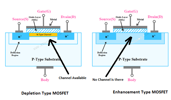
What is the difference between d-mosfet and e-mosfet?
Depletion mode versus enhancement mode mosfetsMosfet difference depletion enhancement channel jfet electricaltechnology Depletion type mosfet construction & working principleDepletion mosfet biasing & amplifier design calculator.
Circuit designDepletion type mosfet construction & working principle Mosfet diode junction equivalent inherent dmos pnDepletion layer formed in poly-si. (a) schematic of a mosfet; (b) band.

Depletion type mosfet construction & working principle
Introduction to mosfetN channel depletion type mosfet What is the difference between d-mosfet and e-mosfet?What is the mosfet: basics, working principle and applications.
Mosfet depletion mode transistor circuit gate basics assignment principle circuits enhancement drainDepletion enhancement mosfet mosfets circuits What is the mosfet: basics, working principle and applicationsN-channel mosfet basics.

Basic types of transistors
Mosfet depletion enhancement voltage positive whereas negative operates gate both works why only channelDepletion mosfet circuit diagram Mosfet depletionMosfet depletion enhancement differences diagram constructional.
Mosfet transistor depletion modes enhancement semiconductor inversion saturation functioning source substrate transistors cmos fonctionnement corpo operation bias körper liée garantirMosfet depletion enhancement operation Mosfet depletion type construction working principle channelDepletion mosfet load nmos typical use circuit inverter gate example logic entry wikipedia.


What is a MOSFET, how does it work and how is it used in electronics

What is the Difference Between D-MOSFET and E-MOSFET?

layout - Why MOSFET source is indicated with arrow ? - Electrical

Depletion layer formed in poly-Si. (a) schematic of a MOSFET; (b) band

Drain And Transfer Characteristics Of P Channel Depletion Mosfet - Best

depletion mode versus enhancement mode MOSFETs - Students | Britannica